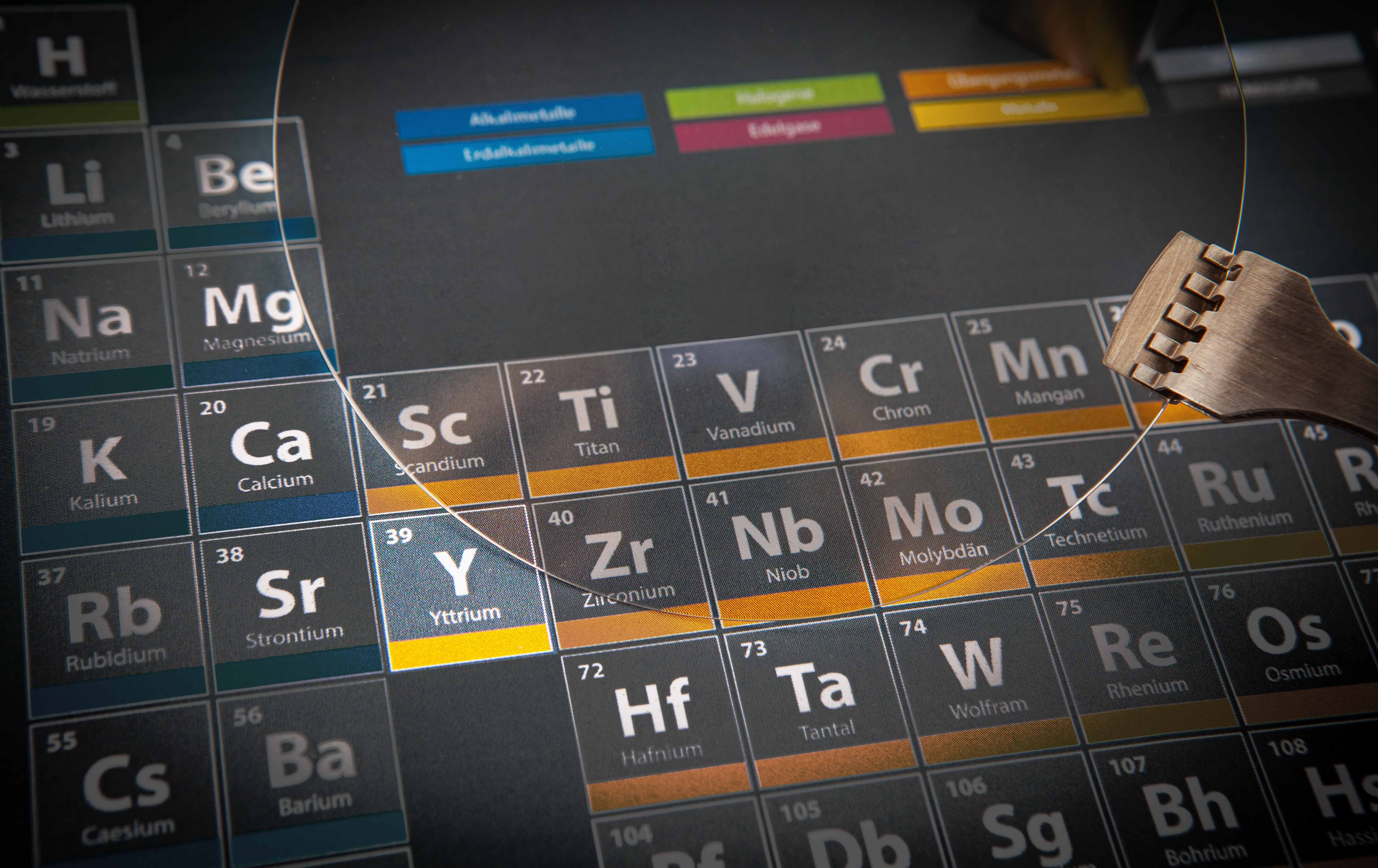
Milestone in semiconductor development
New semiconductor material: AlYN promises more energy-efficient and powerful electronics
Researchers at Fraunhofer IAF have made a breakthrough in the field of semiconductor materials: With aluminum yttrium nitride (AlYN), they have succeeded in fabricating and characterizing a new and promising semiconductor material using the MOCVD process. Due to its excellent material properties and its adaptability to gallium nitride (GaN), AlYN has enormous potential for use in energy-efficient high-frequency and high-performance electronics for information and communications technology.
Aluminum Yttrium Nitride (AlYN) has attracted the interest of many research groups around the world due to its outstanding material properties. However, the growth of the material has been a major challenge. Until now, AlYN could only be deposited by magnetron sputtering. Researchers at the Fraunhofer Institute for Applied Solid State Physics IAF have now succeeded in fabricating the new material using metal-organic chemical vapor deposition (MOCVD) technology, thus enabling the development of new, diverse applications.
“Our research represents a milestone in the development of new semiconductor structures. AlYN is a material that enables increased performance while minimizing energy consumption, paving the way for innovations in electronics that our digitally connected society and its ever-increasing technology demands urgently need,” says Dr. Stefano Leone, scientist at Fraunhofer IAF in the field of epitaxy. With its promising material properties, AlYN could become a key material for future technological innovations.
Recent research had already demonstrated the material properties of AlYN, such as ferroelectricity. In developing the new compound semiconductor, the researchers at Fraunhofer IAF focused primarily on its adaptability to gallium nitride (GaN): The lattice structure of AlYN can be optimally adapted to GaN and the AlYN/GaN heterostructure promises significant advantages for the development of future-oriented electronics.
From layer to heterostructure
In 2023, the Fraunhofer IAF research group achieved groundbreaking results when it succeeded in depositing a 600 nm thick AlYN layer for the first time. The layer with wurtzite structure contained an unprecedented yttrium concentration of more than 30 percent. Now the researchers have achieved another breakthrough: they have fabricated AlYN/GaN heterostructures with a precisely adjustable yttrium concentration, which are characterized by excellent structural quality and electrical properties. The novel heterostructures have an yttrium concentration of up to 16 percent. The structural analysis group, led by Dr. Lutz Kirste, continues to perform detailed analyses to further the understanding of the structural and chemical properties of AlYN.
The Fraunhofer researchers have already measured very promising electrical properties of AlYN that are of interest for use in electronic components. “We were able to observe impressive values for sheet resistance, electron density and electron mobility. These results showed us the potential of AlYN for high-frequency and high-performance electronics,” Leone reports.
AlYN/GaN heterostructures for high-frequency applications
Due to its wurtzite crystal structure, AlYN can be adapted very well to the wurtzite structure of gallium nitride with a suitable composition. An AlYN/GaN heterostructure promises to enable the development of semiconductor components with improved performance and reliability. In addition, AlYN has the ability to induce a two-dimensional electron gas (2DEG) in heterostructures. Recent research results from Fraunhofer IAF show optimal 2DEG properties in AlYN/GaN heterostructures at an yttrium concentration of about 8 percent.
The material characterization results also show that AlYN can be used in high electron mobility transistors (HEMTs). The researchers observed a significant increase in electron mobility at low temperatures (more than 3000 cm2/Vs at 7 K). The team has already made significant progress in demonstrating the epitaxial heterostructure required for fabrication, and continues to explore the new semiconductor for the development of HEMTs.
The researchers are also optimistic about industrial applications: Using AlYN/GaN heterostructures grown on 4-inch SiC substrates, they demonstrated the scalability and structural uniformity of the heterostructures. The successful creation of AlYN layers in a commercial MOCVD reactor enables scaling up to larger substrates in larger MOCVD reactors. This method is considered the most productive for the fabrication of large-area semiconductor structures and underlines the potential of AlYN for the mass production of semiconductor devices.
Development of non-volatile memories
Due to its ferroelectric properties, AlYN is highly suitable for the development of non-volatile memory applications. Another important advantage is that the material has no limitation on layer thickness. Therefore, the research team at Fraunhofer IAF encourages further research into the properties of AlYN layers for non-volatile memories, as AlYN-based memories can drive sustainable and energy-efficient data storage solutions. This is particularly relevant for data centers, which have to cope with the exponential growth in computing capacity for artificial intelligence and have significantly higher energy consumption.
The challenge of oxidation
A major obstacle to the industrial use of AlYN is its susceptibility to oxidation, which affects its suitability for certain electronic applications. “In the future, it will be important to explore strategies to reduce or overcome oxidation. The development of high-purity precursors, the use of protective coatings, or innovative manufacturing techniques could contribute to this. The susceptibility of AlYN to oxidation is a major research challenge to ensure that research efforts are focused on areas with the greatest chance of success,” concludes Leone.
Scientific publications
S. Leone et al. “Metal-Organic Chemical Vapor Deposition of Aluminum Yttrium Nitride”, Phys. Status Solidi RRL 17 2300091 (2023)
https://doi.org/10.1002/pssr.202300091
I. Streicher et al. “Two-dimensional electron gases in AlYN/GaN heterostructures grown by metal–organic chemical vapor deposition”, APL Materials 12 051109 (2024)
https://doi.org/10.1063/5.0203156
The use of the photos is permitted exclusively in connection with this press release and with indication of the copyright.
Last modified:
 Fraunhofer Institute for Applied Solid State Physics IAF