Baden-Württemberg contributes 4.35 million euros in funding as part of the EU Chips Act
Fraunhofer IAF expands technology capabilities for chiplet innovations within the APECS pilot line
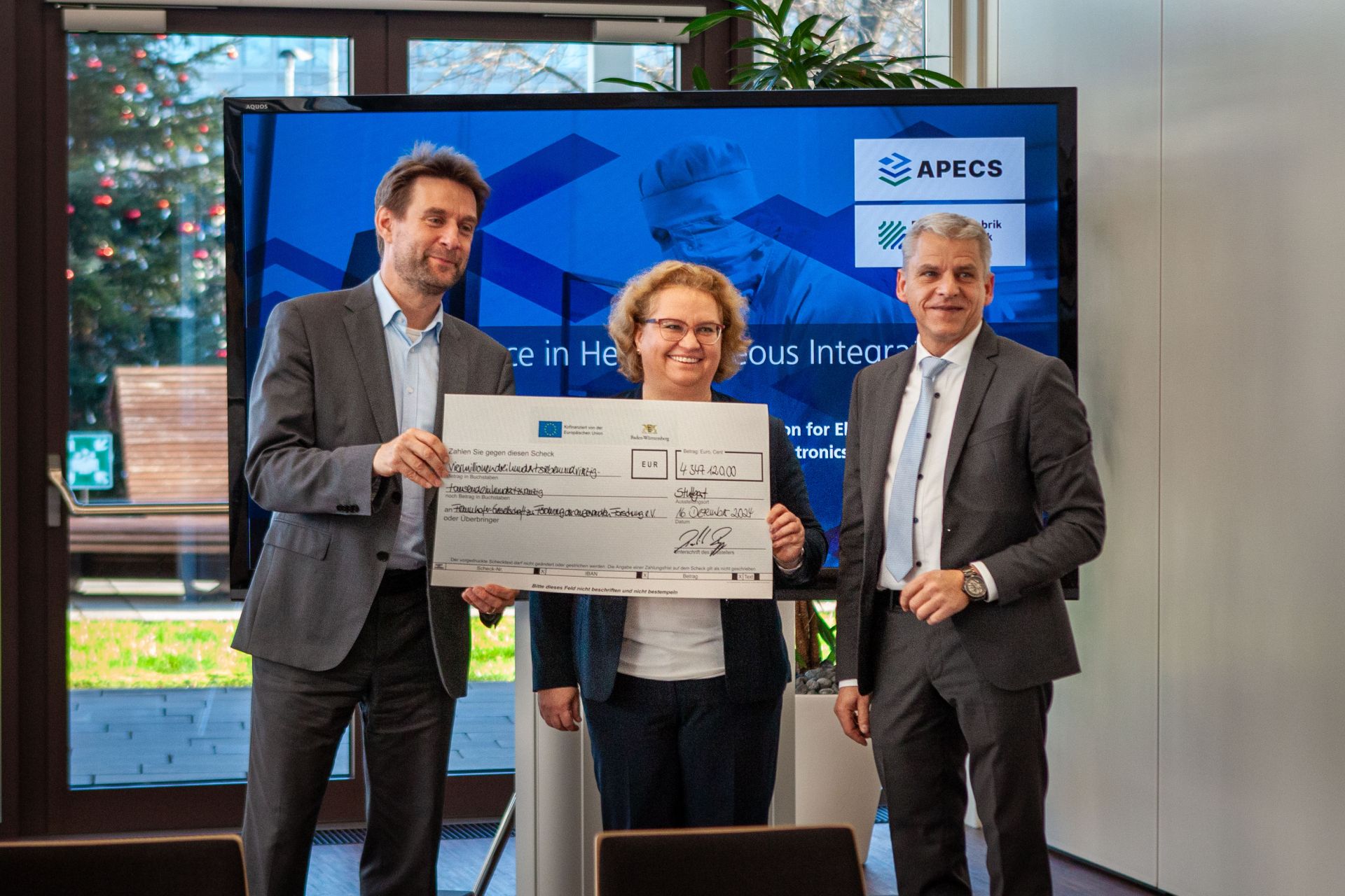
Fraunhofer IAF is expanding its technological capabilities in the field of III-V compound semiconductors, making a valuable contribution to the development of the APECS pilot line within the framework of the EU Chips Act. The Baden-Württemberg Ministry of Economic Affairs, Labour and Tourism is contributing 4.35 million euros to the funding. On 16 December 2024, State Secretary for Economic Affairs Dr. Patrick Rapp symbolically handed over a cheque for the funding amount to the institute’s directors. APECS will make it possible to further expand the research and development infrastructure across Europe over the next 4.5 years. The substantial total funding amounts to 730 million euros, provided by Chips Joint Undertaking, the Federal Ministry of Education and Research (BMBF) and other funding.


As part of the pilot line “Advanced Packaging and Heterogeneous Integration for Electronic Components and Systems” (APECS), the Fraunhofer Institute for Applied Solid State Physics IAF will continue to expand its semiconductor research infrastructure in the coming years. It will receive support from the state of Baden-Württemberg in the form of national funding amounting to 4.35 million euros.
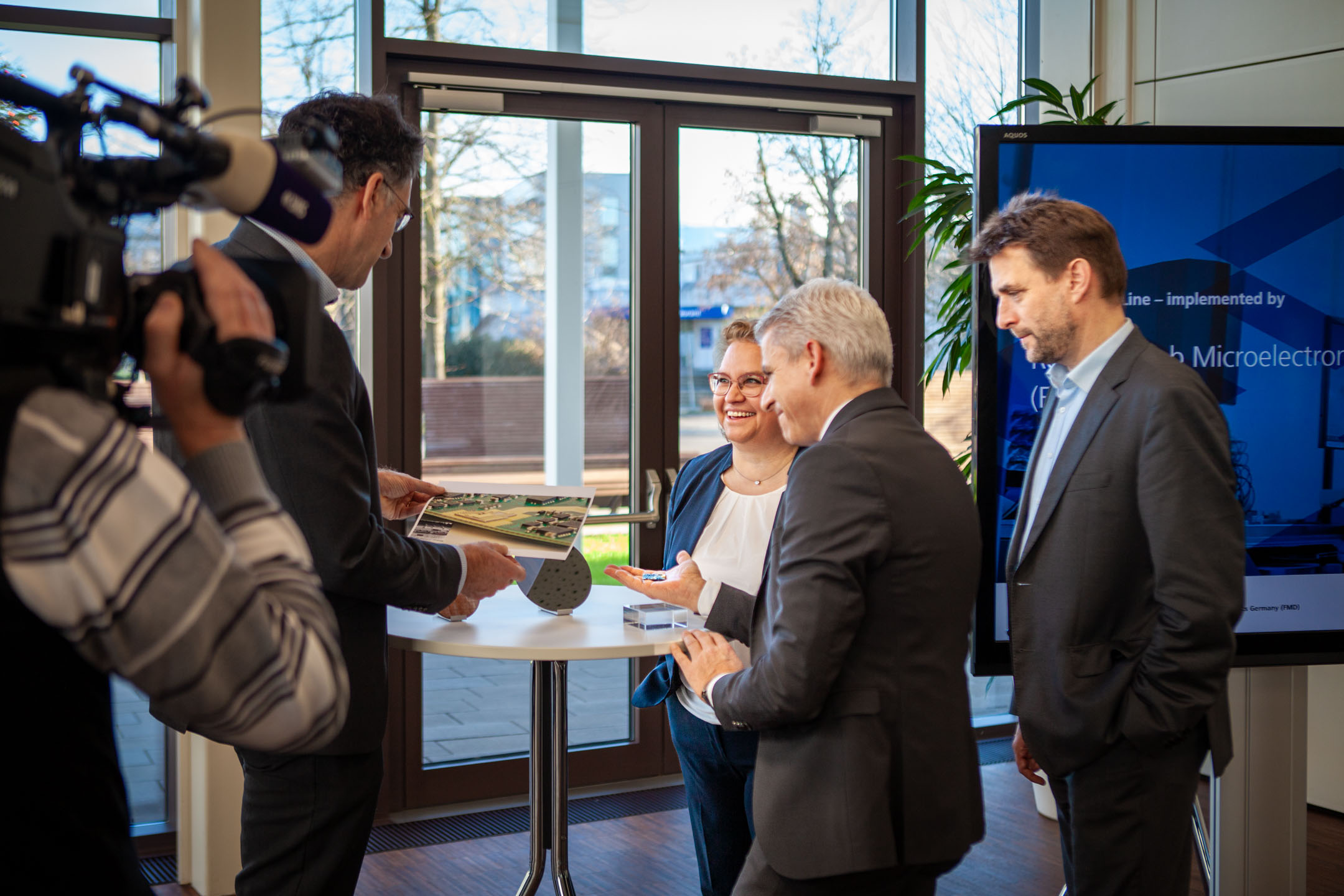
On 16 December 2024, State Secretary Dr. Patrick Rapp from the Baden-Württemberg Ministry of Economic Affairs, Labour and Tourism visited Fraunhofer IAF and symbolically handed over a cheque for the funding amount. Afterwards, the State Secretary for Economic Affairs was informed on site about the planned measures and the APECS pilot line, which will be coordinated by the Fraunhofer-Gesellschaft and implemented by the Research Fab Microelectronics Germany (FMD) over the next 4.5 years.
“The APECS pilot line is a project of strategic importance for Baden-Württemberg, as it is about participating in highly innovative developments in the field of semiconductor technologies and supporting a rapid transfer to our companies. Only in this way can we as a state continue to demonstrate our role as a leading innovation region in Europe,” said Dr. Patrick Rapp, State Secretary in the Ministry of Economic Affairs, Labour and Tourism, at the handover of the symbolic funding cheque.
Strengthening European competitiveness in the development and production of semiconductors
“As a research institute, we can contribute to overcoming the immense challenges that Europe is currently facing. Our innovations can provide valuable impetus for the European economy and contribute to greater competitiveness and resilience in times of crisis. APECS enables us to develop technology in a targeted manner, the benefits of which are available to small and medium-sized enterprises throughout the EU and at the same time strengthen Baden-Württemberg as a business location in the long term. We would like to thank the Baden-Württemberg Ministry of Economic Affairs for its generous support,” explains Dr. Patricie Merkert, who together with Prof. Dr. Rüdiger Quay forms the dual leadership of the Fraunhofer IAF.
Prof. Dr. Quay emphasizes: “APECS will enable us to take several important steps towards the future in one go, both by significantly improving the performance of our research infrastructure and by tapping into key future topics. The further development of our capabilities in heterogeneous integration will pave the way for many new innovations. The upscaling of elementary technologies at our institute brings our processes even closer to the industrial standard. This benefits both our development work and the economy - in the region and in Europe.”
APECS: Heterogeneously integrated technologies for the European economy
The APECS pilot line is an important component of the EU Chips Act to drive chiplet innovation and increase research and manufacturing capacity for semiconductors in Europe. The institutes cooperating in the FMD are working closely with other European partners to set up the pilot line and are thus making a significant contribution to strengthening Europe’s technological resilience and thus also increasing global competitiveness in the semiconductor industry.
The pilot line will provide large industrial companies as well as small and medium-sized enterprises (SMEs) and start-ups with low-threshold access to cutting-edge technologies and ensure secure, resilient semiconductor value chains. APECS is co-funded by Chips Joint Undertaking and by national funding from Austria, Belgium, Finland, France, Germany, Greece, Portugal and Spain under the Chips for Europe initiative. The total funding for the APECS pilot line amounts to EUR 730 million over 4.5 years.
The APECS pilot line focuses on the scalable industrial transfer of newly developed innovations in the field of heterointegration, in particular the use of new chiplet technologies, thus building a bridge to application-oriented research. APECS goes beyond conventional system-in-package (SiP) methods and aims to deliver robust and trustworthy heterogeneous systems that significantly increase the innovative capacity of the European semiconductor industry.


Chiplets for high-frequency applications and production on 6’’ wafers
As an institute cooperating in the FMD, Fraunhofer IAF is developing novel chiplets based on the hybrid semiconductor material systems indium gallium arsenide-on-silicon (InGaAs-on-Si) and gallium nitride-on-silicon carbide (GaN-on-SiC) as well as microbump interposers as part of APECS. These technologies are particularly suitable for high-frequency applications due to their outstanding values in key parameters such as noise, output power and efficiency and promise innovations in measurement technology, communication, radar technology and sensor technology.
“Chiplets offer significant advantages in the development and production of high-performance electronic and optical components, as they enable compact and highly efficient multifunctional systems. The combination of different functions such as control logic and amplifiers on one carrier improves both the performance and energy efficiency of a system. We are very much looking forward to further developing our technologies within the framework of APECS,” explains Dr. Patrick Waltereit, head of the Technology department at Fraunhofer IAF.
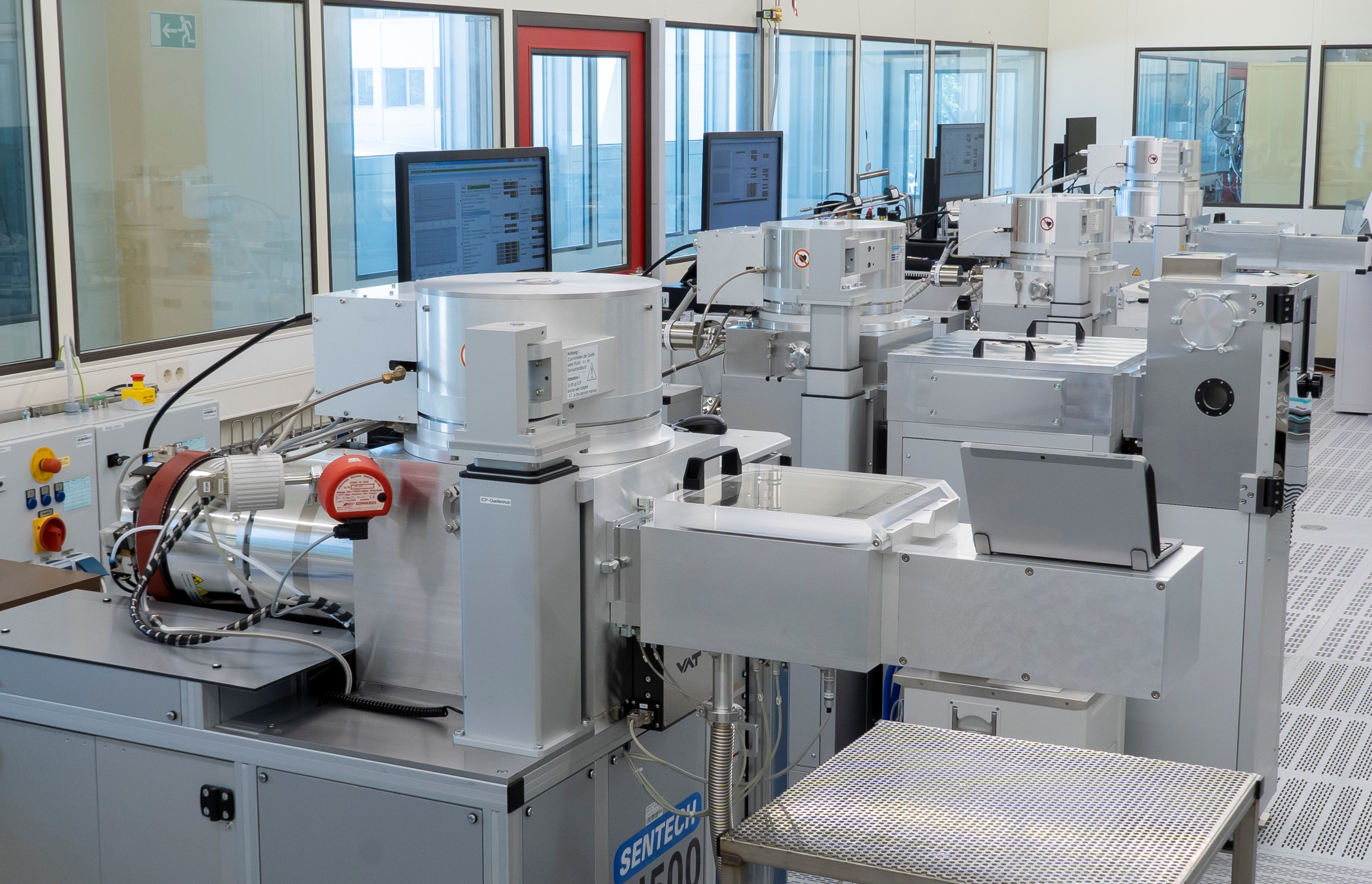
To ensure easy transfer to industry, the development and production of the chiplets and interposers at Fraunhofer IAF will take place on 6’’ wafers. New equipment for epitaxy, process technology and metrology will therefore be procured and put into operation in the institute's clean room. In addition, existing processes for chiplet and interposer production are being adapted.
Chiplets: Integration of individual technologies increases functionality and reduces costs
The increasing performance and cost requirements for electronic components mean that conventional semiconductor chips are increasingly reaching their technological limits. The processing of large integrated circuits, as required for comprehensive functionalities, causes high costs, as individual defects have an extremely strong impact on the yield of a single wafer. In addition, chemical and mechanical incompatibilities between different materials and layer structures mean that only a limited number of different technologies can be implemented on a single wafer.
A novel solution for efficiently increasing system functionality is the electrical or optical connection of individual small components (so-called chiplets) on a common substrate (interposer). With the chiplet approach, the individual technologies can each undergo the optimum epitaxy and processing for them and then form a highly functional, flexible and efficient chip-sized system through low-loss integration. This modularization also increases scalability, simplifies chip design and shortens the time to market for innovations.
Funding
APECS is co-funded by the Chips Joint Undertaking and national funding authorities of Austria, Belgium, Finland, France, Germany, Greece, Portugal, Spain, through the Chips for Europe Initiative.


The use of the photos is permitted exclusively in connection with this press release and with indication of the copyright.
Last modified:
 Fraunhofer Institute for Applied Solid State Physics IAF