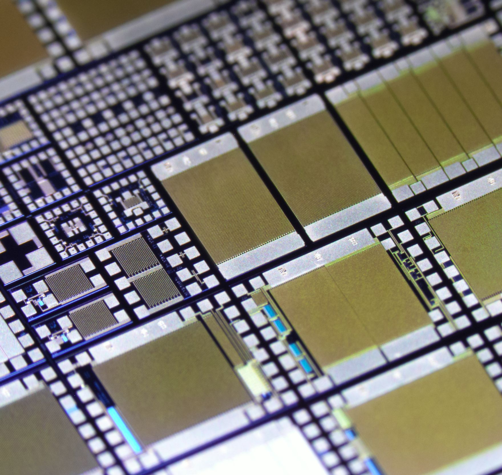
Fraunhofer IAF has joined GaN Valley to contribute its capabilities in high-frequency and power electronics to the development of sovereign European semiconductor supply chains. Networking within the growing ecosystem provides European companies and scientific institutions specializing in GaN with a common platform for in-depth collaboration.
Fraunhofer IAF joins GaN Valley
06/25/2024 / European ecosystem for wide-bandgap semiconductors

The Fraunhofer Institute for Applied Solid State Physics IAF has become a member of GaN Valley. The initiative connects companies and scientific institutions to create a European ecosystem for the sovereign development and manufacturing of devices based on the III-V compound semiconductor gallium nitride (GaN). The aim is to provide members with a platform for knowledge transfer and in-depth cooperation and, on this basis, to establish secure European supply chains for promising GaN technologies.
“We see close cooperation with companies in the EU semiconductor industry and scientific institutions that also specialize in GaN as an important contribution to strengthening the European economy and promoting independence in Europe,” explains Achim Lösch, Business Developer for High Frequency and Power Electronics at Fraunhofer IAF. “With this in mind, we look forward to actively participating in GaN Valley.”
Research and development of GaN devices along the value chain
Fraunhofer IAF contributes its expertise and infrastructure to the initiative for the research and development of novel GaN-based devices, circuits, and modules for applications in power and high-frequency electronics, such as high-bit-rate satellite communication and energy conversion for electric vehicles or heat pumps. Thanks to its high-performance 1000 m2 clean room, the institute is able to offer services along the entire semiconductor value chain, from design, epitaxy, processing, and characterization to module construction and (sub)system integration, both for the development of individual demonstrators and for small series production.
Why GaN?
As a wide-bandgap semiconductor, GaN is characterized by a number of advantages over elemental semiconductors such as silicon (Si). GaN-based circuits suffer lower energy losses, can handle higher voltages and frequencies, and are more robust, e.g., they can be reliably operated at higher ambient temperatures than Si-based circuits.
 Fraunhofer Institute for Applied Solid State Physics IAF