 Fraunhofer Institute for Applied Solid State Physics IAF
Fraunhofer IPMS and IAF collaborate with 34 European partners in project ARCTIC
EU-project joins forces towards the era of scalable control technology for quantum processors
In order to make quantum computers usable, developing the control technology is at least as important for scaled systems, yet it is still in its infancy. Project ARCTIC brings together 36 international partners from industry, academia and leading RTOs to establish a complete and comprehensive European supply chain and develop scalable, reliable, innovative control infrastructure for cryogenic quantum processors. The German Institutes Fraunhofer IPMS and Fraunhofer IAF contribute their extensive expertise in device characterization. The EU is funding the project with over € 11 million for a duration of three years.
Quantum computing is currently seen as the most promising contender to efficiently solve problems which are completely out of reach for classical computers. Such a computer requires an enormous amount of control technology and interfacing to function. For quantum computers based on qubits operated close to absolute zero Kelvin inside a cryostat, the number of possible signal lines fed from the machinery into the cryostat is currently limited due to restricted space, heat exchange through the wires and the signal integrity due to long wires.
“The performance requirements asked of electronic devices and circuits at cryogenic temperatures are quite different compared to those at room temperature. Especially when interfacing very sensitive applications such as quantum processors, all aspects of microelectronic technologies need to be optimized,” says Alexander Grill, scientific leader of ARCTIC (“Advanced Cryogenic Technologies for Innovative Computing”) at Belgian research center imec. The expected project outcomes are considered as important enablers for highly demanded technologies that can resolve existing problems in areas such as computational chemistry, bio and life sciences, cryptography needed for data protection and cyber security.


ARCTIC brings together 36 partners from industry, academia and leading RTOs to establish a complete and comprehensive European supply chain for cryogenic photonics, microelectronics, and cryo-microsystems around the emerging quantum computing industry and different cryo-enabled ICT applications.
Fraunhofer is involved in ARCTIC with its Institutes for Photonic Microsystems IPMS and for Applied Solid State Physics IAF. Their focus within the project lies on the characterization of semiconducting devices in cryogenic environments and peripheral devices for cryogenic quantum computing processors on full wafers as well as the analysis of the electrical behavior of transistors and memory devices at untypically low temperatures.
Fraunhofer IAF characterizes peripheral devices for cryogenic quantum processors
Device characterization is as crucial as it is time-consuming, especially when it comes to cryogenic measurements and characterization with long cool-down and warm-up times. Fraunhofer IAF takes an essential role in ARCTIC by providing characterization capabilities of peripheral devices for cryogenic quantum processors on commercially sized wafers with an automated cryogenic full-wafer prober. Alongside its extensive knowledge in characterization methodologies for semiconductor device for R&D purposes up to industrial tests of 200 mm and 300 mm wafers, Fraunhofer IAF is one of the very few European providers of such low temperatures test set-up below 2 Kelvin. This profound knowledge about cryogenic device characterization and statistical variability of key technologies will be integral to ARCTIC and help accelerate the industrial testing of cryogenic technologies necessary to scale up quantum computing.
The project at Fraunhofer IAF is financed by the EU (Horizon Europe) and co-financed by the German Federal Ministry of Education and Research (BMBF).
Fraunhofer IPMS will contribute competencies in characterization of commercial semiconductor devices
The Center Nanoelectronic Technologies (CNT) at Fraunhofer IPMS focuses on the characterization and modelling of bipolar and CMOS-transistors as well as memory elements at cryogenic temperatures. The emphasis will be put on high frequency, noise and defect characterization and modelling of commercial transistors in 22FDX FDSOI technology as well as the development of optimized non-volatile ferroelectric memories. For this, it is crucial to improve characterization methods in cryogenic environments and on full wafers and to generate a deep understanding of how field-effect transistors and memory devices behave at untypically low temperatures. “We want to gain new insights into the energetic position and number of electrical defects in the transistors. This will allow the industry to offer new cryo-designated products and Fraunhofer to offer unique characterization methodologies for these products. The reduction of defect induced noise in electronics is an important factor for increasing the coherence time of qubit states, that is why the developed methodologies are directly relevant for cryogenic quantum computing approaches. Regarding the non-volatile memories it is furthermore important to minimize the power consumption of the devices, since the cooling power is very limited inside of cryostats” explains Dr. Maik Simon, researcher within the Quantum Technologies group at the CNT in Dresden, Germany.
Another demonstration of Fraunhofer IPMS’s competences is investigating the applicability of non-volatile ferroelectric three-terminal memories for a cryogenic environment by electrical characterization and physical modelling. This pioneering study will reveal how the devices perform at low temperatures and what parameters can be altered to enhance switching characteristics, integration density and reliability.
The project at Fraunhofer IPMS is co-financed by the German Federal Ministry of Education and Research (BMBF) and the Saxon State Ministry for Economic Affairs, Labour and Transport (SMWA).
About ARCTIC
ARCTIC brings together technology developers, technology integrators, modelers, designers, system/application players and end users to ensure a smooth interfacing between respective layers. At the same time, we focus a large fraction of the effort on missing links – among others in the cryo-modelling and standardization space. In addition, we strongly leverage the unique R&D ecosystem in Europe, with RTOs collaborating and forming the bridge between the academic innovation models and the industrial valorization – the latter both at SMEs and large industrial companies at once.
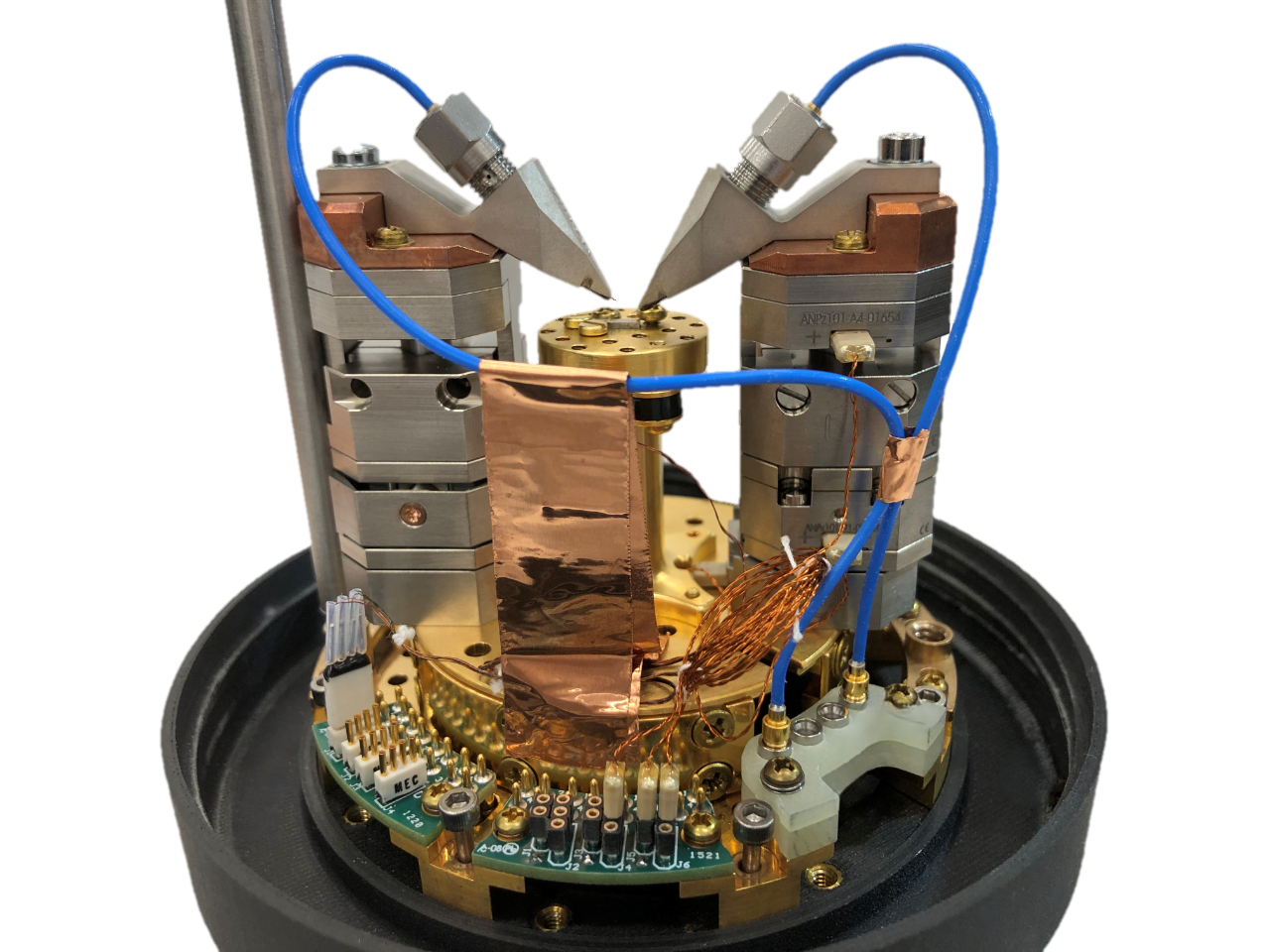
Cryogenic wafer prober

Nikola David Komericki summarizes the features, advantages, and applications of the cryogenic wafer prober for the automated characterization of qubit devices. Fraunhofer IAF has commissioned the facility in 2023.
The use of the photos is permitted exclusively in connection with this press release and with indication of the copyright.
Last modified: